Ask Latest Price
Active Member
8 Years

Shenzhen Jingxin Electronic Technology Co., Ltd.
Shenzhen Jingxin Electronic Technology Co., Ltd.


Add to Cart
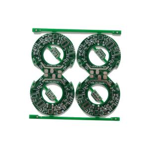
FR4 HTG Material Multi Circuit Boards 4 Layer Blind Via Holes Pcb 2 Years Guarantee
4 layers Multilayer PCB board
* Customized circuit board.
* 100% testing.
* Accept sample and bulk order.
| Product Type | RGD ROHS PCB |
| Material | FR4 |
| Surface finishing | HASL/ENIG/OSP |
| Quote needs | PCB Gerber file |
| Feature | high precision |
| Legend | White |
| Color | Green |
| Board thickness | 1.6mm |
PCB Capacity
| PCB General Capability | |
| Number of Layer | 1 - 18 Layer |
| Maximum Processing Area | 680 × 1000MM |
| Min Board Thickness | 2 Layer - 0.3MM ( 12 mil ) |
| 4 Layer - 0.4MM ( 16 mil ) | |
| 6 Layer - 0.8MM ( 32 mil ) | |
| 8 Layer - 1.0MM ( 40 mil) | |
| 10 Layer - 1.1MM ( 44 mil ) | |
| 12 Layer - 1.3MM ( 52 mil ) | |
| 14 Layer - 1.5MM ( 59 mil ) | |
| 16 Layer - 1.6MM ( 63 mil ) | |
| 18 Layer - 1.8MM ( 71 mil ) | |
| Finished Board Thickness Tolerance | Thickness ≤ 1.0MM, Tolerance: ± 0.1MM |
| 1.0MM ≤ Thickness ≤ 6.5MM, Tolerance ± 10% | |
| Twisting and Bending | ≤ 0.75%, Min: 0.5% |
| Range of TG | 130 - 215 ℃ |
| Impedance Tolerance | ± 10%, Min: ± 5% |
| Hi-Pot Test | Max: 4000V/10MA/60S |
| Surface Treatment | HASL, With Lead, HASL Free Lead |
| Flash Gold, Immersion Gold | |
| Immersion Silver, Immersion Tin | |
| Gold Finger, OSP | |
| PCB Cu Thickness + Plating | |
| Out Layer Cu Thickness | 1 - 6OZ |
| Inner Layer Cu Thickness | 0.5 - 4OZ |
| Cu Thickness of PTH | 20UM ≤ Average ≤ 25UM |
| Min: 18UM | |
| HASL with Lead | Tin 63% Lead 37% |
| HASL Free Lead | 7UM ≤ Surface Thickness ≤ 12UM |
| Thick Gold Plating | Ni Thickness: 3 - 5UM ( 120u" - 200u" ) |
| Gold Thickness: 0.025 - 1.27UM ( 1u" - 50u" ) | |
| Immersion Gold | Ni Thckness: 3 - 5UM ( 120u" - 200u" ) |
| Gold Thickness: 0.025 - 0.15UM ( 1u" - 3u" ) | |
| Immersion Silver | Ag Thickness: 0.15- 0.75 UM ( 6u" - 30u" ) |
| Gold Finger | Ni Thickness: 3 - 5UM ( 120u" - 160u" ) |
| Gold Thickness: 0.025 - 1.51UM ( 1u" - 60u" ) | |
| U940 PCB Pattern Limit Capability | |
| Min Width | 0.075MM ( 3 mil ) |
| Min Trace | 0.075MM ( 3 mil ) |
| Min Width of Ring ( Inner Layer ) | 0.15MM ( 6 mil ) |
| Min Width of Ring ( Out Layer ) | 0.1MM ( 4 mil ) |
| Min Solder Bridge | 0.1MM ( 4 mil ) |
| Min Height of Legend | 0.7MM ( 28 mil ) |
| Min Width of Legend | 0.15MM ( 6 mil ) |
| PCB Holes Processing Capability | |
| Final Hole Size | Min: Laser 0.1MM, Machine 0.2MM |
| Drilling Hole Size | 0.10 - 6.5MM |
| Drilling Tolerance | NPTH: ±0.05MM, PTH: ±0.075MM |
| Final Hole Size Tolerance ( PTH ) | φ0.20 - 1.60MM ± 0.075MM |
| φ1.60 - 6.30MM ± 0.10MM | |
| Final Hole Size Tolerance ( NPTH ) | φ0.20 - 1.60MM ± 0.05MM |
| φ1.60 - 6.50MM ± 0.05MM | |
| Drilling Strip Hole | -0L ~tu.'gth /width 2:1 |
| Min Strip Hole Width 0.65MM | |
| Length & Width Tolerance ± 0.05MM | |
| Board Thickness / Hole Size | ≤ 10:1 |
| PCB Cover Thickness Capability | |
| Solder Mask Color | Green,Matte Green,Yellow,Blue,Red,Black,Matte Black,White |
| Solder Mask Thickness | Surface Line ≥ 10UM |
| Surface Line Corner ≥ 6UM | |
| Surface Board 10 - 25UM | |
| Solder Mask Bridge Width | |
| Legend Color | White,Yellow,Black |
| Min Height of Legend | 0.70MM ( 28 mil ) |
| Min Width of Legend | 0.15MM ( 6 mil ) |
| Blue Gel Thickness | 0.2 - 1.5MM |
| Blue Gel Tolerance | ±0.15MM |
| Carbon Print Thickness | 5 - 25UM |
| Carbon Print Min Space | 0.25MM |
| Carbon Print Impedance | 200Ω |
| Blind/Burried/Half Via PCB Capability | |
| Parameters | (1+1)e.g. (4-layer)blind via:1-2,2-4 (6-layer)buried via:2-3,3-4 (8-layer)blind/buried:1-3,4-5,6-8 |
| Min Via | Laser 0.1MM, Machine 0.2MM |
| Half Via | Min: 0.6MM |
| Impedance Capability | |
| Resistance Value | Single-ended 50 - 75Ω, Difference 100Ω, Coplanar 50 - 75Ω |
Q1: Are you a factory or trade company?
A: We have our own PCB manufacturing & Assembly factory.
Q2: What kind of PCB file format can you accept for production?
A: Gerber, PROTEL 99SE, PROTEL DXP, POWER PCB, CAM350, GCCAM, ODB+(.TGZ)
Q3: Are my PCB files safe when I submit them to you for manufacturing?
A: We respect customer's copyright and will never manufacture PCB for someone else with your files unless we receive written. Permission from you, nor we'll share these files with any other 3rd parties.
Q4: No PCB file/Gbr file, only have the PCB sample,can you produce it for me?
A: Yes,we could help you to clone the PCB. Just send the sample PCB to us, we could clone the PCB design and work out it.
Q5: What is Chuante lead time?
A: Sample:
1-2 Layers: 5 to 7working days
4-8 Layers: 12 working days
Mass production:
1-2 Layers:7 to 15 working days
4-8 Layers:10 to 18 working days
The leadtime is depends on your final confirmed quantity.
Q6: What payment do you accept ?
A: -Wire Transfer(T/T)
-Western Union
-Letter of Credit(L/C)
-Paypal
-Ali Pay
-Credit Cart
Q7: How to get the PCBs?
A: For small packages, we will ship the boards to you by DHL,UPS,FedEx,EMS. Door to door service! You will get your PCBs at your home.
For heavy goods more than 300kg, we may ship your PC boards by ship or by air to save freight cost. Of course, if you have your own forwarder, we may contact them for dealing with your shipment.
Q8: What is your minimum order quantity?
A:Our MOQ is 1 PCS.
Q9: How about your factory production capacity?
A: we can provide 100000 square meter/month.
Q10: Which countries have you worked with?
A: US,Mexico,Korea,Vitnam,Italy,Iran,Bengal and so on we all supplied.
PCB Photos
